

Sign In Join Free


1 / 5
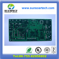
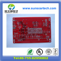
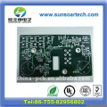
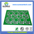
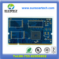
BGA pcb development,PCB layout design


Basic Info
| Model No. | YZX-PCB001 |
|---|
Product description
1.Double-sided PCB circuit board
2.FR4 material
3.Copper thickness:1OZ
4.Finishing board thickness:0.8mm
5.Min hole size:6mil
6.Min line width:0.076mm
7.Min line spacing:0.076mm
8.Surface treatment:OSP,Lead-free and immersion gold
9.Reasonable price+excellent quality+fast delivery
The Urgent service
24 hours for 2-Layer sample
48 hours for 4-Layer sample
72 hours for 6-Layer sample
BGA pcb development,PCB layout design
Send your inquiry to this supplier
You may also be interested in
Product Categories

Product Alert
Subscribe to your interested keywords. We will send freely the latest and hottest products to your Inbox. Don't miss any trade information.
Your use of this website constitutes acknowledgement and acceptance of our Terms & Conditions.
Copyright ? 2009-2026 Bossgoo Co., Ltd. All rights reserved.
