

Sign In Join Free


Video
1 / 8
PCB SMT Assembly Programmable chip processing
$85.00
≥1000 Piece/Pieces
$75.00
≥3000 Piece/Pieces
$65.00
≥5000 Piece/Pieces


Basic Info
| Brand Name | Wtt/Wsd |
|---|
Product description


- 2yrs


- Manufacturer
- Service
- Distributor/Wholesaler
- Other
Video
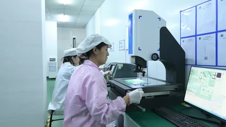
Product Testing
Product Testing
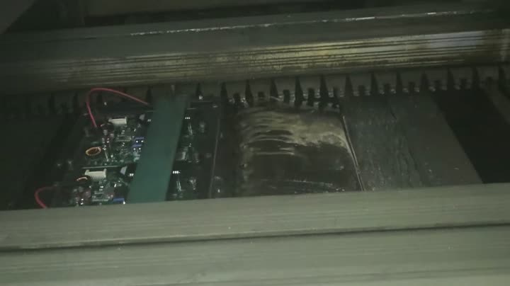
The wave welding peak passes through the furnace in the pcba production process
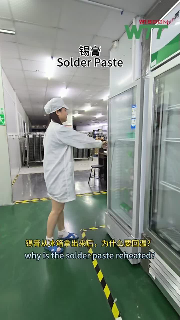
PCB processing is why solder paste can not be used directly
Product Testing
The wave welding peak passes through the furnace in the pcba production process
PCB processing is why solder paste can not be used directly
PCB SMT Assembly Programmable chip processing
$85.00
≥1000 Piece/Pieces
$75.00
≥3000 Piece/Pieces
$65.00
≥5000 Piece/Pieces
Send your inquiry to this supplier
You may also be interested in
- Printed circuit board
- Blank Printed Circuit Board
- printed circuit board design
- printed circuit board prototyp
- Printed circuit board recyclin
- flexible printed circuit board
- unitech printed circuit board
- Printed Circuit Board Assembly
- Printed Circuit Board Pen
- Printed Circuit Board Silver
- fpc printed circuit board
- double printed circuit board
- Printed Circuit Board Tape
- of printed circuit board
- Printed Circuit Board PCB
Product Categories


Product Alert
Subscribe to your interested keywords. We will send freely the latest and hottest products to your Inbox. Don't miss any trade information.
Your use of this website constitutes acknowledgement and acceptance of our Terms & Conditions.
Copyright ? 2009-2026 Bossgoo Co., Ltd. All rights reserved.
